 The use of infrared thermography in electronics and electrical industry allows contactless measurement of surface temperatures with an infrared camera without contacting temperature sensors. It is an elegant, non-invasive optical temperature measurement method for simultaneous and temporally high-resolution detection of a number of measurement points.
The thermographic inspection of electronic components and assemblies is an established test procedure for failure detection and quality management – from the development of first prototypes to serial production. This enables, for example, the following to be detected:
- Hotspots and atypical temperature distributions on the surface of printed circuit boards, integrated circuits and multichip modules
- Increased contact resistances
- Increased resistance due to constriction of wires
- Hidden cracks in joints
- Power losses due to RF mismatch
- Incorrect thermal connections of heat sinks
- Short circuits, soldering defects such as cold solder joints
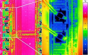 Thermographic analysis during each development step provides important conclusions for the optimisation of heat management and the design of complex electronic assemblies. In electronics production thermographic temperature measurement is used as a versatile instrument for quality assurance. High-performance thermography has become indispensable for setting critical technological parameters and their permanent monitoring as well as for inline testing of products in the production process and their final functional test.
Further Characteristics of the Use of Thermography in Electrical Engineering and Electronics
- Influences neither the RF impedance of the measurement object nor the heat dissipation of the same, which serves the safe avoidance of corresponding measurement errors
- Allows safe temperature measurement even on live working parts
- Complete recording of the temperature distribution and its temporal course of complex assemblies
- Highest spatial resolution by using measurement systems with detectors with a very high number of pixels and opto-mechanical MicroScan unit
- Resolution of smallest geometrical structures using close up lenses and infrared microscope lenses
- Detection of smallest temperature differences using cooled photon detectors and lock-in measurement methods
- Easy-to-use analysis and documentation of measurement results with powerful analysis software
Advantages when Using Powerful Thermographic Systems
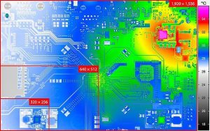
– Detector resolutions up to (1,920 × 1,536) native IR pixels for testing complex assemblies
– Capturing of high-resolution detail images with pixel sizes up to < 1 μm using specific microscopic lenses
– Detection of temperature differences between defective and intact structures in the range of a few micro-Kelvin due to high thermal resolution up to < 0.015 K in combination with the lock-in method
 – Measurement accuracy of up to ± 1 °C or 1 % for accurate measurement results
Individual Configuration of Thermographic Systems for Electronics and Electrical Engineering
Depending on the respective task, users can get the equipment configured meeting their specific needs. The starting point will usually be the thermographic camera. Cooled or uncooled detector? Which detector format? Shall the thermographic system support lock-in thermography? How much flexibility is desired for the distance between the measurement object and the camera? What influence does this have on the choice of microscopic lenses and close-ups? Depending on what the answers to these questions will be, InfraTec can offer thermographic systems of various performance levels – from the individual camera to the automated modular E-LIT test bench.
Electronic / Semiconductor Testing Solution – E-LIT
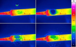
E-LIT – Lock-In Thermography for electronics is an automated testing solution system (as part of NDT techniques) which allows non-contact (electrical) failure analysis of semiconductor material during the manufacturing process. Inhomogeneous temperature distribution, local power loss, leakage currents, resistive vias, cold joints, latch-up effects and soldering issues can be measured with Lock-in Thermography. This is achieved by using the shortest measurement times combined with a high-performance thermographic camera and a specialised lock-in procedure.
 The power supply for this process is clocked with a synchronization module and failures that produce mK or even μK temperature differences are reliably detected by the Lock-in Thermography system.
Smallest defects at electronic components like point and line shunts, issues from overheating, internal (ohmic) shorts, oxide defects, transistor and diode failures on a PCB surface, in integrated circuits (IC´s), LED modules and battery cells can be detected and displayed in x and y positions. Additionally, it is possible to analyse stacked-die packages or multi-chip modules in z-direction with merely changing the lock-in frequency.
The powerful Lock-in Thermography software uses the latest algorithms and routines from most recent scientific publications.
E-LIT is extremely powerful also in resolving smallest geometrical structures as it can be equipped with strong microscopic lenses and additional SIL lenses. Identifying smallest structures with InfraTec´s E-LIT does not mean that the resulting field of view will also be smallest – implementing thermal cameras with detector sizes of up to (1,920 x 1,536) pixels provide large scale microscopic imaging. For even larger imaging stitching options are available.
Discover more at www.qd-uki.co.uk